
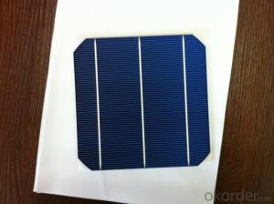
Mono Solar Cells156mm*156mm in Bulk Quantity Low Price Stock
- Ref Price:
-

- Loading Port:
- Shanghai
- Payment Terms:
- TT OR LC
- Min Order Qty:
- 10000 pc
- Supply Capability:
- 100000 pc/month
OKorder Service Pledge
OKorder Financial Service
You Might Also Like


Item specifice
Brief Introduction
- Up to 20.0% efficiency, one of the highest performing mono crystalline cells on the market
- Three bus bars boosts current collection over the entire cell area, leading to higher fill factors
- Blue anti-reflecting coating allows more sunlight be captured and converted to electricity
- Finer, closer fingers improves charge collections for improved energy yield
- Lower light-induced degradation leads to greater power output over the entire module lifetime
- All solar cells are tightly classified to optimize output of module
- Maximum yield and longevity due to hotspot prevention
- Premium appearance results in a highly uniform and aesthetically appealing module
Specification
- Product Mono-crystalline silicon solar cell
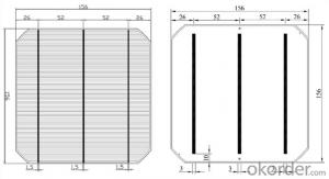
- Dimension 156 mm x 156 mm ± 0.5 mm
- Thickness 200 μm ± 30 μm
- Front 1.5 ± 0.1 mm busbar (silver)
- Silicon nitride antireflection coating
- Back 3.0 mm continuous soldering pads (silver)
- Back surface field (aluminum)
Electric performance parameters

- Testing conditions: 1000 W/m2, AM 1.5, 25 °C, Tolerance: Efficiency ± 0.2% abs., Pmpp ±1.5% rel.
- Imin : at 0.5 V
Light Intensity Dependence

Soldering Ability
- Peel Strength: > 1.0 N/mm (Pull soldered ribbon from busbar in 5 mm/s of 180°)
Dimension Figure

Quick Response
- Any time and anywhere, reply clients' email and solve all problems happen in the work at the first time.
- Remove clients doubts and offer the best solution at the first time.
- Give our clients the lastest news of the photovoltaic, update the newest stock informtion.
Production and Quality Control
- Precision cell efficiency sorting procedures
- Stringent criteria for color uniformity and appearance
- Reverse current and shunt resistance screening
- ISO9001,ISO14001 and OHSAS 18001,TUV Certificated


FAQ:
1. Q: Do you have your own factory?
A: Yes, we have. Our factory located in Jiangsu
2. Q: How can I visit your factory?
A: Before you visit,please contact us.We will show you the route or arrange a car to pick you up.
3. Q: Do you provide free sample?
A: Commenly we provide paid sample.
4. Q: Could you print our company LOGO on the nameplate and package?
A: Yes, we accept it.And need an Authorization Letter from you.
5. Q: Do you accept custom design on size?
A: Yes, if the size is reasonable.
6. Q: How can I be your agent in my country?
A: Please leave feedback. It's better for us to talk about details by email.
7. Q: Do you have solar project engineer who can guide me to install system?
A: Yes, we have a professional engineer team. They can teach you how to install a solar system.
- Q:In the silicon surface cleaning, there is a final step, the silicon chip into the 4% concentration of HF solution soak for five minutes, to hydrogen passivation treatment, and then rinse with deionized water after nitrogen drying,What is the role and mechanism of this hydrogen passivation?
- 0.5 ~ 1min in order to achieve the effect of removing the damage layer, at this timeCorrosion rate can reach 6 to 10um/min.In the polishing process to remove the damage layer on the basis to try to reduce, to prevent corrosion of the wafer was too thin.
- Q:What is the role of emitter diffusion in solar silicon wafers?
- The role of emitter diffusion in solar silicon wafers is to create a region with a high concentration of dopants, typically phosphorus or boron, on the surface of the wafer. This region acts as a junction with the base layer, creating a built-in electric field that separates the generated electron-hole pairs. It facilitates the efficient collection of electrons and holes, leading to improved electrical conductivity and increased solar cell efficiency.
- Q:Can solar silicon wafers be used in off-grid lighting systems?
- Yes, solar silicon wafers can be used in off-grid lighting systems. These wafers are the main component of solar panels, which convert sunlight into electricity. By harnessing solar energy, off-grid lighting systems can operate independently from the traditional power grid, making them ideal for remote or unconnected locations.
- Q:What is the expected lifetime of a solar silicon wafer?
- The expected lifetime of a solar silicon wafer varies depending on several factors such as its quality, manufacturing process, and usage conditions. Generally, high-quality silicon wafers used in solar panels are designed to have a long operational lifespan. They can typically last anywhere from 25 to 30 years or even more with proper maintenance.
- Q:What is the role of solar silicon wafers in reducing air pollution?
- Solar silicon wafers play a crucial role in reducing air pollution by enabling the production of clean and renewable energy through solar panels. These wafers are made from purified silicon, which is a key component in photovoltaic cells. When sunlight hits the silicon wafer, it generates electricity without emitting harmful pollutants like greenhouse gases or particulate matter. By harnessing solar energy, we can reduce our reliance on fossil fuels and decrease air pollution from traditional power sources, ultimately contributing to a cleaner and healthier environment.
- Q:What is the role of a solar silicon wafer in a solar cell?
- The role of a solar silicon wafer in a solar cell is to serve as the substrate or base material on which the photovoltaic (PV) cells are built. The wafer acts as a platform for the formation of the solar cell's semiconductor layers, which are responsible for converting sunlight into electricity. The silicon material used in the wafer possesses unique properties that make it an ideal choice for solar cells, such as its ability to efficiently absorb and convert solar energy. Ultimately, the solar silicon wafer plays a crucial role in enabling the production of renewable and sustainable energy through solar cells.
- Q:For solar wafer cutting diamond wire, what are the characteristics?
- 2, the glass can not be used as the bearing plate of the crystal rod, if the use of graphite plate, grinding down the silicon powder containing a certain amount of graphite, it is difficult to deal with the recovery of silica fume.3, can only be used for single crystal cutting.4, the cost problem. Now the price of diamond wire fell faster, diamond wire cutting costs should be close to the cost of cutting free abrasive.
- Q:How does the efficiency of a solar silicon wafer change over time?
- The efficiency of a solar silicon wafer tends to decrease over time due to various factors such as aging, exposure to environmental conditions, and potential degradation of the materials. This can result in a gradual decline in the wafer's ability to convert sunlight into electricity, leading to a decrease in overall efficiency. Regular maintenance and monitoring can help mitigate this decline and ensure optimal performance over the lifespan of the wafer.
- Q:Can solar silicon wafers be used in solar-powered air conditioning systems?
- Yes, solar silicon wafers can be used in solar-powered air conditioning systems. Silicon wafers are commonly used in solar panels to convert sunlight into electricity, which can then be used to power various appliances, including air conditioning systems.
- Q:How much is the thickness of the silicon wafer
- Around 0.670mm. Wafer must be thinned, otherwise the loss of dicing knife
1. Manufacturer Overview |
|
|---|---|
| Location | |
| Year Established | |
| Annual Output Value | |
| Main Markets | |
| Company Certifications | |
2. Manufacturer Certificates |
|
|---|---|
| a) Certification Name | |
| Range | |
| Reference | |
| Validity Period | |
3. Manufacturer Capability |
|
|---|---|
| a)Trade Capacity | |
| Nearest Port | |
| Export Percentage | |
| No.of Employees in Trade Department | |
| Language Spoken: | |
| b)Factory Information | |
| Factory Size: | |
| No. of Production Lines | |
| Contract Manufacturing | |
| Product Price Range | |
Send your message to us
Mono Solar Cells156mm*156mm in Bulk Quantity Low Price Stock
- Ref Price:
-
- Loading Port:
- Shanghai
- Payment Terms:
- TT OR LC
- Min Order Qty:
- 10000 pc
- Supply Capability:
- 100000 pc/month
OKorder Service Pledge
OKorder Financial Service
Similar products


New products
Hot products


Hot Searches
Related keywords

