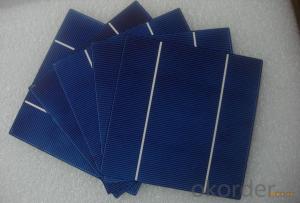


High Current Solar Cell 18.0% Polycrystalline Silicon Solar Cell Price
- Ref Price:
-

- Loading Port:
- Shanghai
- Payment Terms:
- TT OR LC
- Min Order Qty:
- 1000 pc
- Supply Capability:
- 100000 pc/month
OKorder Service Pledge
OKorder Financial Service
You Might Also Like


4 Bus Bars 156*156 17.6% efficiency poly solar cell
PHYSICAL CHARACTERISTICS
Dimension: 156mm x 156mm ± 0.5mm
Wafer Thickeness: 180um+20um and 200um+20um
Front(-) Four 1.2mm silver busbar
Silicon nitride blue anti-reflection coating
Back(+) aluminum back surface field
1.75mm(silver) wide segment soldering pads

Typical Electrical Characteristics
Efficiency | W(Pmpp) | V(Umpp) | A(Impp) | V(Uoc) | A(Isc) |
17.4-17.5 | 4.234 | 0.517 | 8.231 | 0.622 | 8.759 |
17.5-17.6 | 4.259 | 0.519 | 8.243 | 0.623 | 8.769 |
17.7-17.8 | 4.283 | 0.521 | 8.256 | 0.625 | 8.779 |
17.8-17.9 | 4.307 | 0.523 | 8.268 | 0.626 | 8.788 |
17.9-18.0 | 4.332 | 0.525 | 8.281 | 0.627 | 8.798 |
18.0-18.1 | 4.380 | 0.529 | 8.306 | 0.629 | 8.808 |
18.1-18.2 | 4.405 | 0.531 | 8.318 | 0.632 | 8.818 |
18.2-18.3 | 4.429 | 0.533 | 8.331 | 0.633 | 8.837 |
18.3-18.4 | 4.453 | 0.535 | 8.344 | 0.634 | 8.847 |
18.4-18.5 | 4.478 | 0.537 | 8.356 | 0.636 | 8.856 |
18.5-18.6 | 4.502 | 0.539 | 8.369 | 0.637 | 8.866 |
Efficiency | W(Pmpp) | V(Umpp) | A(Impp) | V(Uoc) | A(Isc) |
20.90-21.00 | 5.06 | 0.557 | 9.007 | 0.653 | 9.688 |
20.80-20.90 | 5.04 | 0.556 | 9.062 | 0.652 | 9.683 |
20.70-20.80 | 5.02 | 0.554 | 9.055 | 0.651 | 9.684 |
20.60-20.70 | 4.99 | 0.552 | 9.033 | 0.651 | 9.672 |
20.50-20.60 | 4.97 | 0.550 | 9.002 | 0.650 | 9.673 |
20.40-20.50 | 4.94 | 0.548 | 9.012 | 0.649 | 9.674 |
20.30-20.40 | 4.92 | 0.546 | 9.009 | 0.649 | 9.655 |
20.20-20.30 | 4.89 | 0.543 | 9.012 | 0.648 | 9.634 |
20.10-20.20 | 4.87 | 0.541 | 8.998 | 0.648 | 9.617 |
20.00-20.10 | 4.85 | 0.540 | 8.977 | 0.647 | 9.600 |
*Data under standard testing conditional (STC):1,000w/m2,AM1.5, 25°C , Pmax:Positive power tolerance.
3 Bus Bars 156*156 17.4% efficiency poly solar cell
Dimension: 156 mm x 156 mm ± 0.5 mm
Wafer Thickeness: 156 mm x 156 mm ± 0.5 mm

Typical Electrical Characteristics:
| Efficiency code | 1660 | 1680 | 1700 | 1720 | 1740 | 1760 | 1780 | 1800 | 1820 | 1840 | 1860 |
| Efficiency (%) | 16.6 | 16.8 | 17.0 | 17.2 | 17.4 | 17.6 | 17.8 | 18.0 | 18.2 | 18.4 | 18.6 |
| Pmax (W) | 4.04 | 4.09 | 4.14 | 4.19 | 4.23 | 4.28 | 4.33 | 4.38 | 4.43 | 4.48 | 4.53 |
| Voc (V) | 0.612 | 0.615 | 0.618 | 0.621 | 0.624 | 0.627 | 0.629 | 0.63 | 0.633 | 0.635 | 0.637 |
| Isc (A) | 8.42 | 8.46 | 8.51 | 8.56 | 8.61 | 8.65 | 8.69 | 8.73 | 8.77 | 8.81 | 8.84 |
| Imp (A) | 7.91 | 7.99 | 8.08 | 8.16 | 8.22 | 8.27 | 8.33 | 8.38 | 8.43 | 8.48 | 8.53 |
* Testing conditions: 1000 W/m2, AM 1.5, 25 °C, Tolerance: Efficiency ± 0.2% abs., Pmpp ±1.5% rel.
* Imin : at 0.5 V
Production:

Package:

FAQ:
1. Q: Do you have your own factory?
A: Yes, we have. Our factory located in Jiangsu
2. Q: How can I visit your factory?
A: Before you visit,please contact us.We will show you the route or arrange a car to pick you up.
3. Q: Do you provide free sample?
A: Commenly we provide paid sample.
4. Q: Could you print our company LOGO on the nameplate and package?
A: Yes, we accept it.And need an Authorization Letter from you.
5. Q: Do you accept custom design on size?
A: Yes, if the size is reasonable.
6. Q: How can I be your agent in my country?
A: Please leave feedback. It's better for us to talk about details by email.
7. Q: Do you have solar project engineer who can guide me to install system?
A: Yes, we have a professional engineer team. They can teach you how to install a solar system.
- Q:What are the reasons for the emergence of the black chip phenomenon of the monocrystalline silicon, which aspects of the production process have an impact on it, preventive measures, and improvement measures?
- You say the phenomenon called flower piece, the formation of many factors, the main reason is that contamination, because in the process, the wafer surface after polishing the silicon atom is bond breaking, it is easy to adsorb metal ions and cannot completely by cleaning out.
- Q:Are solar silicon wafers affected by electromagnetic interference (EMI)?
- Solar silicon wafers are not directly affected by electromagnetic interference (EMI). However, the performance of solar panels, which use these wafers, can be influenced by EMI. EMI can interfere with the proper functioning of the electrical components in a solar system, such as inverters or charge controllers, leading to reduced efficiency or even system failure. Therefore, while silicon wafers themselves are not affected, precautions need to be taken to minimize the impact of EMI on the overall solar power system.
- Q:What is the purpose of a grounding wire in a solar silicon wafer?
- The purpose of a grounding wire in a solar silicon wafer is to provide a safe path for electrical currents to flow in the event of a fault or malfunction. It helps to prevent electric shocks, fires, and damage to equipment by redirecting any excess electrical current directly to the ground, ensuring the safety of both the solar wafer and the surrounding environment.
- Q:What is the role of light trapping in solar silicon wafers?
- The role of light trapping in solar silicon wafers is to increase the absorption of sunlight within the wafer, thereby enhancing the overall efficiency of the solar cell. By incorporating light trapping structures or techniques, such as textured surfaces or anti-reflective coatings, more light is effectively captured and confined within the wafer, allowing for a greater number of photons to be converted into electricity. This improves the performance of the solar cell by maximizing the utilization of available sunlight.
- Q:Can solar silicon wafers be repaired if damaged?
- No, solar silicon wafers cannot be repaired if they are damaged. Once a silicon wafer used for solar cells is damaged, it cannot be fixed or repaired. It is usually more cost-effective and efficient to replace the damaged wafer with a new one.
- Q:What is the role of back surface field on solar silicon wafers?
- The back surface field on solar silicon wafers plays a crucial role in enhancing the overall efficiency of solar cells. It acts as a reflective layer that helps to prevent the recombination of charge carriers at the back surface of the wafer. This reduces the loss of current and improves the collection of photons, resulting in higher power output from the solar cell. Additionally, the back surface field also aids in reducing the surface recombination velocity, which further enhances the performance and stability of the solar cell.
- Q:How are solar silicon wafers affected by potential-induced degradation?
- Solar silicon wafers are adversely affected by potential-induced degradation (PID). PID occurs when high voltage potential is applied to the module, leading to a decrease in performance and efficiency. This degradation is primarily caused by the migration of ions, such as sodium, from the glass surface to the silicon wafer, resulting in increased leakage currents and reduced power output. To mitigate PID, various measures like using anti-PID modules or implementing appropriate system grounding techniques are employed in solar panel installations.
- Q:How do defects affect the efficiency of a solar silicon wafer?
- Defects in a solar silicon wafer can significantly affect its efficiency. These defects, such as impurities or structural abnormalities, can reduce the overall performance of the solar cell by hindering the flow of electrons or creating recombination centers. This leads to a decrease in the conversion of sunlight into electricity, resulting in a lower energy output. Therefore, minimizing defects is crucial for ensuring optimal efficiency in solar silicon wafers.
- Q:How are solar silicon wafers protected from physical damage?
- Solar silicon wafers are protected from physical damage through a combination of encapsulation and packaging techniques. The wafers are typically coated with a thin layer of protective material, such as glass or polymer, to shield them from external forces, moisture, and temperature variations. Additionally, they are often laminated between layers of transparent materials, such as tempered glass or polymer films, to provide further protection against impacts, scratches, and environmental degradation. This encapsulation process ensures that the delicate silicon wafers remain intact and functional throughout their lifespan.
- Q:Are solar silicon wafers affected by electromagnetic fields?
- Yes, solar silicon wafers can be affected by electromagnetic fields. Electromagnetic fields can induce eddy currents in the wafers, leading to resistive losses and reduced efficiency in solar cell performance. However, the impact of electromagnetic fields on solar silicon wafers is generally minimal as solar cells are designed to minimize such effects and maintain their functionality.
1. Manufacturer Overview |
|
|---|---|
| Location | |
| Year Established | |
| Annual Output Value | |
| Main Markets | |
| Company Certifications | |
2. Manufacturer Certificates |
|
|---|---|
| a) Certification Name | |
| Range | |
| Reference | |
| Validity Period | |
3. Manufacturer Capability |
|
|---|---|
| a)Trade Capacity | |
| Nearest Port | |
| Export Percentage | |
| No.of Employees in Trade Department | |
| Language Spoken: | |
| b)Factory Information | |
| Factory Size: | |
| No. of Production Lines | |
| Contract Manufacturing | |
| Product Price Range | |
Send your message to us
High Current Solar Cell 18.0% Polycrystalline Silicon Solar Cell Price
- Ref Price:
-
- Loading Port:
- Shanghai
- Payment Terms:
- TT OR LC
- Min Order Qty:
- 1000 pc
- Supply Capability:
- 100000 pc/month
OKorder Service Pledge
OKorder Financial Service
Similar products


New products
Hot products


Hot Searches
Related keywords

