

High Current Solar Cell 17.6% Polycrystalline Silicon Solar Cell Price
- Ref Price:
-

- Loading Port:
- Shanghai
- Payment Terms:
- TT OR LC
- Min Order Qty:
- 1000 pc
- Supply Capability:
- 100000 pc/month
OKorder Service Pledge
OKorder Financial Service
You Might Also Like


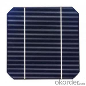
4 Bus Bars 156*156 17.6% efficiency poly solar cell
PHYSICAL CHARACTERISTICS
Dimension: 156mm x 156mm ± 0.5mm
Wafer Thickeness: 180um+20um and 200um+20um
Front(-) Four 1.2mm silver busbar
Silicon nitride blue anti-reflection coating
Back(+) aluminum back surface field
1.75mm(silver) wide segment soldering pads

Typical Electrical Characteristics
Efficiency | W(Pmpp) | V(Umpp) | A(Impp) | V(Uoc) | A(Isc) |
17.4-17.5 | 4.234 | 0.517 | 8.231 | 0.622 | 8.759 |
17.5-17.6 | 4.259 | 0.519 | 8.243 | 0.623 | 8.769 |
17.7-17.8 | 4.283 | 0.521 | 8.256 | 0.625 | 8.779 |
17.8-17.9 | 4.307 | 0.523 | 8.268 | 0.626 | 8.788 |
17.9-18.0 | 4.332 | 0.525 | 8.281 | 0.627 | 8.798 |
18.0-18.1 | 4.380 | 0.529 | 8.306 | 0.629 | 8.808 |
18.1-18.2 | 4.405 | 0.531 | 8.318 | 0.632 | 8.818 |
18.2-18.3 | 4.429 | 0.533 | 8.331 | 0.633 | 8.837 |
18.3-18.4 | 4.453 | 0.535 | 8.344 | 0.634 | 8.847 |
18.4-18.5 | 4.478 | 0.537 | 8.356 | 0.636 | 8.856 |
18.5-18.6 | 4.502 | 0.539 | 8.369 | 0.637 | 8.866 |
Efficiency | W(Pmpp) | V(Umpp) | A(Impp) | V(Uoc) | A(Isc) |
20.90-21.00 | 5.06 | 0.557 | 9.007 | 0.653 | 9.688 |
20.80-20.90 | 5.04 | 0.556 | 9.062 | 0.652 | 9.683 |
20.70-20.80 | 5.02 | 0.554 | 9.055 | 0.651 | 9.684 |
20.60-20.70 | 4.99 | 0.552 | 9.033 | 0.651 | 9.672 |
20.50-20.60 | 4.97 | 0.550 | 9.002 | 0.650 | 9.673 |
20.40-20.50 | 4.94 | 0.548 | 9.012 | 0.649 | 9.674 |
20.30-20.40 | 4.92 | 0.546 | 9.009 | 0.649 | 9.655 |
20.20-20.30 | 4.89 | 0.543 | 9.012 | 0.648 | 9.634 |
20.10-20.20 | 4.87 | 0.541 | 8.998 | 0.648 | 9.617 |
20.00-20.10 | 4.85 | 0.540 | 8.977 | 0.647 | 9.600 |
*Data under standard testing conditional (STC):1,000w/m2,AM1.5, 25°C , Pmax:Positive power tolerance.
3 Bus Bars 156*156 17.4% efficiency poly solar cell
Dimension: 156 mm x 156 mm ± 0.5 mm
Wafer Thickeness: 156 mm x 156 mm ± 0.5 mm

Typical Electrical Characteristics:
| Efficiency code | 1660 | 1680 | 1700 | 1720 | 1740 | 1760 | 1780 | 1800 | 1820 | 1840 | 1860 |
| Efficiency (%) | 16.6 | 16.8 | 17.0 | 17.2 | 17.4 | 17.6 | 17.8 | 18.0 | 18.2 | 18.4 | 18.6 |
| Pmax (W) | 4.04 | 4.09 | 4.14 | 4.19 | 4.23 | 4.28 | 4.33 | 4.38 | 4.43 | 4.48 | 4.53 |
| Voc (V) | 0.612 | 0.615 | 0.618 | 0.621 | 0.624 | 0.627 | 0.629 | 0.63 | 0.633 | 0.635 | 0.637 |
| Isc (A) | 8.42 | 8.46 | 8.51 | 8.56 | 8.61 | 8.65 | 8.69 | 8.73 | 8.77 | 8.81 | 8.84 |
| Imp (A) | 7.91 | 7.99 | 8.08 | 8.16 | 8.22 | 8.27 | 8.33 | 8.38 | 8.43 | 8.48 | 8.53 |
* Testing conditions: 1000 W/m2, AM 1.5, 25 °C, Tolerance: Efficiency ± 0.2% abs., Pmpp ±1.5% rel.
* Imin : at 0.5 V
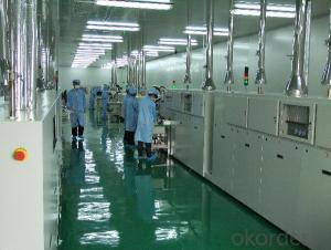
Production:

Package:

FAQ:
1. Q: Do you have your own factory?
A: Yes, we have. Our factory located in Jiangsu
2. Q: How can I visit your factory?
A: Before you visit,please contact us.We will show you the route or arrange a car to pick you up.
3. Q: Do you provide free sample?
A: Commenly we provide paid sample.
4. Q: Could you print our company LOGO on the nameplate and package?
A: Yes, we accept it.And need an Authorization Letter from you.
5. Q: Do you accept custom design on size?
A: Yes, if the size is reasonable.
6. Q: How can I be your agent in my country?
A: Please leave feedback. It's better for us to talk about details by email.
7. Q: Do you have solar project engineer who can guide me to install system?
A: Yes, we have a professional engineer team. They can teach you how to install a solar system.
- Q:What is the role of rear surface passivation in solar silicon wafers?
- The role of rear surface passivation in solar silicon wafers is to reduce the recombination of charge carriers at the rear surface of the wafer, thereby improving the overall efficiency of the solar cell. Passivation helps to prevent the loss of electrons and holes, allowing them to be collected and utilized for electricity generation.
- Q:Can solar silicon wafers be used in concentrated photovoltaic systems?
- Yes, solar silicon wafers can be used in concentrated photovoltaic systems. These systems use lenses or mirrors to concentrate sunlight onto smaller areas of solar cells, which can be made using silicon wafers. This concentration helps increase the efficiency of the photovoltaic system by focusing more sunlight onto the solar cells and generating more electricity.
- Q:How long does a solar silicon wafer typically last?
- A solar silicon wafer typically lasts for several decades, with an average lifespan ranging from 25 to 30 years.
- Q:Can solar silicon wafers be reused or repurposed after their lifespan in a solar panel?
- Yes, solar silicon wafers can be reused or repurposed after their lifespan in a solar panel. While they may no longer be suitable for generating electricity in solar panels, these wafers can be recycled to extract valuable materials such as silicon, silver, and glass. The extracted materials can then be used in various industries, including electronics, semiconductors, and glass manufacturing, promoting a more sustainable approach to resource utilization.
- Q:How does the efficiency of a solar silicon wafer vary with different angles of sunlight?
- The efficiency of a solar silicon wafer typically varies with different angles of sunlight. As the angle of sunlight changes, the amount of solar energy reaching the surface of the wafer also changes. Generally, the efficiency tends to decrease as the angle of sunlight deviates from perpendicular (90 degrees) to the wafer's surface. This decrease occurs because the solar energy is spread over a larger area, reducing the intensity of the light absorbed by the silicon material. Therefore, it is important to optimize the orientation and tilt of solar panels to maximize their efficiency by capturing sunlight at the most favorable angles throughout the day.
- Q:How are solar silicon wafers connected in a solar panel?
- Solar silicon wafers are typically connected in a solar panel through a process called stringing and tabbing. In this process, the wafers are interconnected using thin conductive wires or ribbons, known as busbars, which create a series circuit. These busbars are soldered onto the front and back contacts of the wafers, allowing for the flow of electricity between them. This interconnected network of wafers forms the photovoltaic module or solar panel.
- Q:How does the thickness of a front contact affect the efficiency of a solar silicon wafer?
- The thickness of a front contact on a solar silicon wafer can affect its efficiency. A thicker front contact can reduce the amount of light reaching the silicon wafer, leading to lower efficiency. However, a thinner front contact can result in higher resistance and increased electrical losses, also impacting efficiency. Therefore, finding the optimal thickness that balances light absorption and electrical performance is crucial for maximizing the efficiency of a solar silicon wafer.
- Q:How much energy is needed to produce a solar silicon wafer?
- The amount of energy required to produce a solar silicon wafer can vary depending on several factors such as the manufacturing process, technology used, and efficiency of the production facility. However, on average, it is estimated that around 250-350 kilowatt-hours (kWh) of energy are needed to manufacture one square meter of a standard silicon wafer for solar panels.
- Q:Can solar silicon wafers be used in solar-powered water desalination systems?
- Yes, solar silicon wafers can be used in solar-powered water desalination systems. The silicon wafers are typically used in solar panels to convert sunlight into electricity, which can then power the water desalination process.
- Q:Can solar silicon wafers be used in disaster response vehicles?
- Yes, solar silicon wafers can be used in disaster response vehicles. These wafers can be integrated into the vehicle's design to harness solar energy and provide power for various equipment and systems, such as lighting, communication devices, and charging stations. This allows the vehicle to operate independently from traditional power sources and ensures continuous operation during disasters or remote locations where power supply may be disrupted.
1. Manufacturer Overview |
|
|---|---|
| Location | |
| Year Established | |
| Annual Output Value | |
| Main Markets | |
| Company Certifications | |
2. Manufacturer Certificates |
|
|---|---|
| a) Certification Name | |
| Range | |
| Reference | |
| Validity Period | |
3. Manufacturer Capability |
|
|---|---|
| a)Trade Capacity | |
| Nearest Port | |
| Export Percentage | |
| No.of Employees in Trade Department | |
| Language Spoken: | |
| b)Factory Information | |
| Factory Size: | |
| No. of Production Lines | |
| Contract Manufacturing | |
| Product Price Range | |
Send your message to us
High Current Solar Cell 17.6% Polycrystalline Silicon Solar Cell Price
- Ref Price:
-
- Loading Port:
- Shanghai
- Payment Terms:
- TT OR LC
- Min Order Qty:
- 1000 pc
- Supply Capability:
- 100000 pc/month
OKorder Service Pledge
OKorder Financial Service
Similar products


New products

Hot products


Hot Searches
Related keywords

