

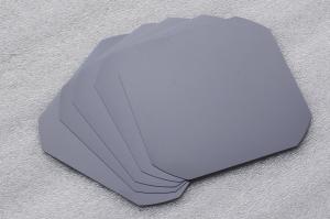
Monocrystalline Solar Silicon Wafer
- Ref Price:
-

- Loading Port:
- Shanghai Port
- Payment Terms:
- TT or LC
- Min Order Qty:
- 100Pieces PCS
- Supply Capability:
- 700 MW/Per Year PCS/month
OKorder Service Pledge
OKorder Financial Service
You Might Also Like


Specification of Mono Silicon Wafers
We can provide you solar wafer both156*156 and 125*125mm, Mono and Poly
Solar Wafers for your raw materials choice.
| Product name | Mono Wafer |
| Conductive type | P type |
| Square size wafer(mm) | 156×156±0.5 |
| Resistivity range | 1~3 ohm |
| Corner(mm) | 150±0.5;165±0.5 |
| 195±0.5;200±0.5 | |
| Thickness (μm) | 200±20 |
| Total thickness(um) | ≤ 30 |
| Resistivity range(Ωcm) | 1-3 |
| Doping elements | Boron |
| Orientation | (100)±1° |
| Carbon content(atoms/cc) | ≤1.0E+17 |
| Oxygen content(atoms/cc) | ≤1.0E+18 |
| Lifetime(μs) | ≥10 |
| Surface quality | No crack, gap, missing Angle, perforated, silicon fell and stress |
| Warping degrees(warp/μm) | ≤50 |
| Neighbouring vertical degree | 90±0.5° |
| Side damage(mm) | ≤0.5mm(length)×0.3mm(width)(not more than 2 per wafer) |
| Line mark(μm) | ≤15 |
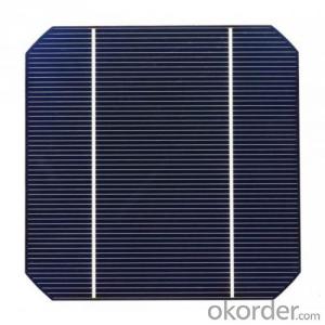
Usage and Applications of Mono Solar Wafers
Mono Solar Wafers mainly used in Solar Cells with reliable quality and trustful efficiency performance. Our Wafers should be your best choice for raw materials.
Packaging & Delivery of Mono Solar Wafers
Carton Box Package and Deliver by air. It should be avoid of moist, water and shaking to protect the safety of Solar Cells.
Factory Picture of Mono Solar Wafers

Package Picture of Mono Solar Wafers

- Q:How efficient are solar silicon wafers in converting sunlight into electricity?
- Solar silicon wafers are highly efficient in converting sunlight into electricity. On average, they have a conversion efficiency of around 15-20%, with some advanced technologies achieving efficiencies above 25%. This means that a significant portion of the incoming sunlight is converted into usable electrical energy, making solar silicon wafers a reliable and effective choice for harnessing solar power.
- Q:Can solar silicon wafers be used in floating solar power plants?
- Yes, solar silicon wafers can be used in floating solar power plants. These floating solar power plants are designed to harness solar energy by placing photovoltaic panels on floating platforms on water bodies such as lakes, reservoirs, or even the ocean. The solar silicon wafers serve as the main component of the photovoltaic panels, converting sunlight into electricity. Floating solar power plants offer numerous advantages, including increased efficiency due to the cooling effect of the water and the ability to utilize unused water surfaces, making solar silicon wafers a suitable choice for such installations.
- Q:The process for steel wire cutting silicon factory, we use HCTB5 wire, you can do?
- Product advantages of electroplated diamond wireCurrent line cutting methodInternal cuttingThe material utilization rate is only 40%~50%, and there are many defects, such as the wide kerf, the lower material, the poor precision of the surface shape, the depth of the surface damage layer and the size of the workpiece being machined.
- Q:Can solar silicon wafers be used in solar-powered wearable devices?
- Yes, solar silicon wafers can be used in solar-powered wearable devices. The wafers can be integrated into the design of wearable devices such as smartwatches, fitness trackers, or even clothing, to harness sunlight and convert it into electrical energy to power the device.
- Q:How does the efficiency of a solar silicon wafer vary with different angles of sunlight?
- The efficiency of a solar silicon wafer varies with different angles of sunlight. The ideal angle for maximum efficiency is when the sunlight is perpendicular to the surface of the wafer. As the angle deviates from perpendicular, the efficiency decreases. This is because the photons have to travel a longer distance through the silicon material, resulting in higher chances of absorption and scattering, thus reducing the overall conversion of sunlight into electricity.
- Q:How to extract silicon from silicon wafers
- Chamfer: the annealed silicon wafer is trimmed into an arc shape, which can prevent the wafer edge from cracking and lattice defect, and increase the flatness of the epitaxial layer and the photoresist layer. In this process, the silica fume is produced by water leaching to produce waste water and silicon slag. [1]
- Q:Can solar silicon wafers be used in marine or offshore applications?
- Yes, solar silicon wafers can be used in marine or offshore applications. However, special considerations need to be taken into account to ensure their durability and protection against harsh marine environments, such as corrosion resistance and waterproofing. Additionally, marine or offshore solar installations may require specific mounting and anchoring techniques to withstand the challenges posed by waves, saltwater, and high winds.
- Q:How are solar silicon wafers protected from environmental factors?
- Solar silicon wafers are protected from environmental factors through various measures. One common method is the use of anti-reflective coatings, which not only reduce reflection but also protect the surface of the wafer from dust, moisture, and other contaminants. Additionally, a passivation layer is applied to the surface to prevent oxidation and enhance the electrical properties of the wafer. The wafer is typically encapsulated within a durable and weather-resistant material, such as tempered glass or a polymer, which shields it from physical damage and provides insulation against temperature variations and moisture. This encapsulation is further reinforced by a frame or module structure to ensure long-term protection against environmental factors.
- Q:How does the efficiency of a solar silicon wafer change with air pollution?
- The efficiency of a solar silicon wafer decreases with increased air pollution. Air pollutants such as dust, smog, and particulate matter can accumulate on the surface of the wafer, reducing its ability to absorb sunlight and convert it into electricity. Additionally, pollutants can cause shading, reducing the amount of sunlight reaching the wafer. Therefore, maintaining clean air is essential to maximize the efficiency of solar silicon wafers.
- Q:How is a solar silicon wafer connected to other components in a solar panel?
- A solar silicon wafer is typically connected to other components in a solar panel through a series of electrical connections. These connections are made using conductive materials, such as metal ribbons or wires, which are soldered to the front and back contacts of the wafer. The ribbons or wires are then connected to the junction box of the solar panel, allowing for the transfer of electrical current generated by the wafer to other components, such as the inverter or battery, for further use or storage.
1. Manufacturer Overview |
|
|---|---|
| Location | |
| Year Established | |
| Annual Output Value | |
| Main Markets | |
| Company Certifications | |
2. Manufacturer Certificates |
|
|---|---|
| a) Certification Name | |
| Range | |
| Reference | |
| Validity Period | |
3. Manufacturer Capability |
|
|---|---|
| a)Trade Capacity | |
| Nearest Port | |
| Export Percentage | |
| No.of Employees in Trade Department | |
| Language Spoken: | |
| b)Factory Information | |
| Factory Size: | |
| No. of Production Lines | |
| Contract Manufacturing | |
| Product Price Range | |
Send your message to us
Monocrystalline Solar Silicon Wafer
- Ref Price:
-
- Loading Port:
- Shanghai Port
- Payment Terms:
- TT or LC
- Min Order Qty:
- 100Pieces PCS
- Supply Capability:
- 700 MW/Per Year PCS/month
OKorder Service Pledge
OKorder Financial Service
Similar products


New products

Hot products


Hot Searches
Related keywords

