
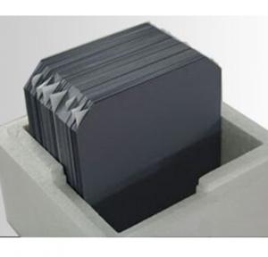


Solar Mono Silicon Wafer for Solar Cell (156 and 125)
- Ref Price:
-

- Loading Port:
- China main port
- Payment Terms:
- TT or LC
- Min Order Qty:
- 10000 pc
- Supply Capability:
- 1000000 pc/month
OKorder Service Pledge
OKorder Financial Service
You Might Also Like


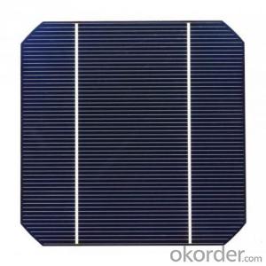
1. Structure of Solar Mono Silicon Wafer for Solar Cell (156 and 125) Description
A wafer, also called a slice or substrate, is a thin slice of semiconductor material, such as acrystalline silicon, used in electronics for the
fabrication of integrated circuits and in photovoltaics for conventional, wafer-based solar cells. The wafer serves as the substrate for
microelectronic devices built in and over the wafer and undergoes many microfabrication process steps such as doping or ion
implantation,etching, deposition of various materials, and photolithographic patterning. Finally the individual microcircuits are separated
(dicing) and packaged.
2. Main Features of the Solar Mono Silicon Wafer for Solar Cell (156 and 125)
• High quality Silicon wafer carrier box
• quartz glass wafer carrier from Taifulong Technology
3. Solar Mono Silicon Wafer for Solar Cell (156 and 125) Images
")
")
4. Solar Mono Silicon Wafer for Solar Cell (156 and 125) Specification
窗体顶端 Item窗体底端 | N-type solar grade mono silicon wafer(125x125mm) | N-type solar grade mono silicon wafer(156x156mm) |
Growth Method | CZ | CZ |
Conductive Type | N-type | N-type |
Dopant | Phos. | Phos. |
Orientation | <100>±3° | <100>±3° |
Resistivity | 1 –3,3-6Ω•cm | 1 –3,3-6 Ω•cm |
Bulk Lifetime | ≥1000μs | ≥1000μs |
Oxygen Content | ≤0.1*1018 cm3 | ≤0.1*1018 cm3 |
Carbon Content | ≤0.1*1017 /cm3 | ≤0.1*1017 /cm3 |
Dimension | 125*125±0.5mm | 156*156±0.5mm |
Diagonal | 150±0.5mm | 200±0.5mm |
Square Sides Angle | 90±0.3° | 90±0.3° |
Thickness | 200±20 um | 200±20 um |
TTV | ≤25um | ≤25um |
Saw Mark | ≤15um | ≤15um |
Warp | ≤40um | ≤40um |
Chips | Depth<0.3mm;Length<0.5mm | Depth<0.3mm;Length<0.5mm, |
less than 2chips per wafer | less than 2chips per wafer | |
Appearance | No Stain, No Pinhole and Cracks by Visual Inspection | No Stain, No Pinhole and Cracks by Visual Inspection |
Dislocation Density | ≤1000 pcs/cm2 | ≤1000 pcs/cm2 |
Package | Packed in Polyethylene foam box,400pcs/box | Packed in Polyethylene foam box,400pcs/box 窗体底端 |
5. FAQ of Solar Mono Silicon Wafer for Solar Cell (156 and 125)
Q1. How long can we receive the product after purchase?
A1.In the purchase of product within three working days, We will arrange the factory delivery as soon as possible. The pecific time of receiving is related to the state and position of customers
Q2. Can we visit your factory?
A2:Surely, I will arrange the trip basing on your business schedule.
Q3:Which payment terms can you accept?
A3:T/T,L/C,Moneygram,Paypal are available for us.
- Q:What are the potential future advancements in solar silicon wafer technology?
- Some potential future advancements in solar silicon wafer technology include the development of thinner and more efficient wafers, advancements in multi-junction solar cells, improvements in manufacturing processes, and the integration of silicon wafer technology with other materials such as perovskites or tandem cells. Additionally, research is being conducted to enhance the stability and durability of silicon wafers, increase their flexibility for use in various applications, and explore new methods for reducing production costs. Overall, the future of solar silicon wafer technology holds promise for higher efficiency, improved performance, and wider adoption of solar energy.
- Q:How long does a solar silicon wafer typically last?
- A solar silicon wafer typically has a lifespan of around 25 to 30 years.
- Q:How are solar silicon wafers cleaned and maintained?
- Solar silicon wafers are cleaned and maintained through a multi-step process. First, any loose dirt or debris is removed by gently brushing or rinsing the surface. Next, a mild detergent or specialized cleaning solution is applied to remove stubborn dirt or oily residues. The wafers are then rinsed with deionized water to ensure no residue is left behind. Finally, the wafers are dried using clean, lint-free cloths or by air-drying. Regular inspections and maintenance, such as checking for any cracks or damages, are also essential to ensure optimal performance of the solar silicon wafers.
- Q:Can solar silicon wafers be used in solar-powered transportation systems?
- Yes, solar silicon wafers can be used in solar-powered transportation systems. They are commonly used in the production of solar panels, which can be installed on vehicles to harness solar energy and power the transportation systems.
- Q:I am not learning electricity, the problem is not professional please understandFor example, in the past, we are in the physics of the secondary wire or wire that is connected to the resistance in the integrated circuit is how to reflect? I know it is the use of lithography technology, is not equivalent to the formation of a line into a line (corrosion into the groove)? And then connect the resistors and capacitors
- And for why it's cheaper to use silicon, it's not because of its semiconductor nature that it uses it. The formation of P and N, a multi hole, a multi electron, and thus the role of different doping. GaAs expensive, but the performance is good, mostly for high-speed circuits and military aspects.
- Q:Why should the wafer cut side, cut out edge Jiaosha
- To determine the crystal, cutting the adhesive carbon or glass, mounted on the fixed equipment.In simple terms is to determine the crystal direction, in order to facilitate future cutting, design graphics to consider this point, and then ask a little deeper, it is necessary to look at the book.Transistors in general with 111 sides, MOS general 110The reason for this is related to doping, corrosion and other post production, but also the activity of different layers of electrons is different, potential energy is not the same.
- Q:What is the role of solar silicon wafers in promoting energy independence at the community level?
- Solar silicon wafers play a crucial role in promoting energy independence at the community level by serving as the key component in solar photovoltaic (PV) panels. These wafers are responsible for converting sunlight into electricity, enabling communities to generate their own clean and renewable energy. By harnessing solar power, communities can reduce their dependence on traditional fossil fuel sources, contribute to a greener environment, and potentially save on energy costs. Solar silicon wafers are instrumental in empowering communities to take control of their energy needs and contribute towards a more sustainable future.
- Q:What is the typical lifetime energy yield of a solar silicon wafer?
- The typical lifetime energy yield of a solar silicon wafer varies depending on various factors such as the efficiency of the solar cells, the geographical location, and the maintenance of the solar panel system. On average, a solar silicon wafer can generate enough energy to offset its initial embodied energy within 1-4 years. Over its lifetime, a solar silicon wafer can produce around 10-20 times more energy than was used in its manufacturing process.
- Q:Consult the difference between silicon and battery
- From the silicon wafer to the battery piece needs to undergo the process of making wool, and the single crystal silicon wafer is generally made of alkali. Therefore, the appearance of monocrystalline silicon battery is black, and the appearance of polycrystalline silicon sheet is dark blue.
- Q:How is a power output measured in a solar silicon wafer?
- The power output of a solar silicon wafer is typically measured by connecting it to a load resistance and measuring the voltage and current generated by the wafer. The power output is then calculated by multiplying the voltage and current values.
1. Manufacturer Overview |
|
|---|---|
| Location | |
| Year Established | |
| Annual Output Value | |
| Main Markets | |
| Company Certifications | |
2. Manufacturer Certificates |
|
|---|---|
| a) Certification Name | |
| Range | |
| Reference | |
| Validity Period | |
3. Manufacturer Capability |
|
|---|---|
| a)Trade Capacity | |
| Nearest Port | |
| Export Percentage | |
| No.of Employees in Trade Department | |
| Language Spoken: | |
| b)Factory Information | |
| Factory Size: | |
| No. of Production Lines | |
| Contract Manufacturing | |
| Product Price Range | |
Send your message to us
Solar Mono Silicon Wafer for Solar Cell (156 and 125)
- Ref Price:
-
- Loading Port:
- China main port
- Payment Terms:
- TT or LC
- Min Order Qty:
- 10000 pc
- Supply Capability:
- 1000000 pc/month
OKorder Service Pledge
OKorder Financial Service
Similar products


New products
Hot products


Hot Searches
Related keywords

