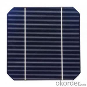


Mono Solar Cells156mm*156mm in Bulk Quantity Low Price Stock 19.6
- Ref Price:
-

- Loading Port:
- Shanghai
- Payment Terms:
- TT OR LC
- Min Order Qty:
- 1000 pc
- Supply Capability:
- 100000 pc/month
OKorder Service Pledge
OKorder Financial Service
You Might Also Like


Brief Introduction
- Up to 20.0% efficiency, one of the highest performing mono crystalline cells on the market
- Three bus bars boosts current collection over the entire cell area, leading to higher fill factors
- Blue anti-reflecting coating allows more sunlight be captured and converted to electricity
- Finer, closer fingers improves charge collections for improved energy yield
- Lower light-induced degradation leads to greater power output over the entire module lifetime
- All solar cells are tightly classified to optimize output of module
- Maximum yield and longevity due to hotspot prevention
- Premium appearance results in a highly uniform and aesthetically appealing module
Specification
- Product Mono-crystalline silicon solar cell
- Dimension 156 mm x 156 mm ± 0.5 mm
- Thickness 200 μm ± 30 μm
- Front 1.5 ± 0.1 mm busbar (silver)
- Silicon nitride antireflection coating
- Back 3.0 mm continuous soldering pads (silver)
- Back surface field (aluminum)
Electric performance parameters

- Testing conditions: 1000 W/m2, AM 1.5, 25 °C, Tolerance: Efficiency ± 0.2% abs., Pmpp ±1.5% rel.
- Imin : at 0.5 V
Light Intensity Dependence

Soldering Ability
- Peel Strength: > 1.0 N/mm (Pull soldered ribbon from busbar in 5 mm/s of 180°)
Dimension Figure

Quick Response
- Any time and anywhere, reply clients' email and solve all problems happen in the work at the first time.
- Remove clients doubts and offer the best solution at the first time.
- Give our clients the lastest news of the photovoltaic, update the newest stock informtion.
Production and Quality Control
- Precision cell efficiency sorting procedures
- Stringent criteria for color uniformity and appearance
- Reverse current and shunt resistance screening
- ISO9001,ISO14001 and OHSAS 18001,TUV Certificated


FAQ:
1. Q: Do you have your own factory?
A: Yes, we have. Our factory located in Jiangsu
2. Q: How can I visit your factory?
A: Before you visit,please contact us.We will show you the route or arrange a car to pick you up.
3. Q: Do you provide free sample?
A: Commenly we provide paid sample.
4. Q: Could you print our company LOGO on the nameplate and package?
A: Yes, we accept it.And need an Authorization Letter from you.
5. Q: Do you accept custom design on size?
A: Yes, if the size is reasonable.
6. Q: How can I be your agent in my country?
A: Please leave feedback. It's better for us to talk about details by email.
7. Q: Do you have solar project engineer who can guide me to install system?
A: Yes, we have a professional engineer team. They can teach you how to install a solar system.
- Q:How are solar silicon wafers connected in a solar array?
- Solar silicon wafers are typically connected in a solar array using soldering or conductive adhesive materials. The wafers are electrically interconnected by soldering or attaching metal ribbons or busbars to their contacts, creating a series of parallel connections. This series of interconnected wafers forms a solar cell module, which is then further connected to other modules to create a larger solar array.
- Q:The metal in the silicon wafer
- By 1960, the scale of industrial production had been in this way. Silicon rectifier and thyristor has prompted the silicon material production jumped in the first semiconductor material. With the development of silicon epitaxial single crystal technology and silicon planar technology in 60s, it not only makes silicon transistor manufacturing technology mature, but also promotes the rapid development of integrated circuits. In early 80s the world's polysilicon production reached 2500 tons. Silicon is one of the promising materials for solar cells. The technology of producing solar cells with polycrystalline silicon has been mature; amorphous silicon films have been developed rapidly. Chemical element silicon. Electrically active impurities phosphorus and boron should be less than 0.4ppb and 0.1ppb in qualified semiconductor and polysilicon. A certain amount of electroactive impurities should be added to the single crystal to obtain the required conductivity and resistivity. Heavy metals such as copper, gold, iron and nonmetal are very harmful impurities. The carbon content in silicon is higher than that of 1ppm. When the carbon content is over 3ppm, the harmful effect is more significant. Oxygen content in silicon is very high. Oxygen is both beneficial and harmful. The content of oxygen in Czochralski silicon is within the range of 5 to 40ppm, and the oxygen content of the fused silica can be less than 1ppm.
- Q:What is a silicon chip made of?
- The main process: polycrystalline silicon - zone melting or direct pulling - single crystal silicon rod - rolling, cutting, grinding, throwing - silicon wafer.
- Q:Can solar silicon wafers be used in solar-powered water treatment plants?
- Yes, solar silicon wafers can be used in solar-powered water treatment plants. These wafers are commonly used in photovoltaic panels to convert sunlight into electricity. In a solar-powered water treatment plant, the solar silicon wafers can be utilized to generate the necessary energy to power the treatment processes, such as filtration, disinfection, and desalination.
- Q:What is the typical voltage output of a solar silicon wafer?
- The typical voltage output of a solar silicon wafer can vary depending on factors such as the size of the wafer, the efficiency of the solar cells, and the intensity of sunlight. However, a typical voltage output range for a single solar silicon wafer is around 0.5 to 0.6 volts.
- Q:How does the thickness of a front contact affect the efficiency of a solar silicon wafer?
- The thickness of a front contact on a solar silicon wafer can affect its efficiency. A thicker front contact can reduce the amount of light reaching the silicon wafer, leading to lower efficiency. However, a thinner front contact can result in higher resistance and increased electrical losses, also impacting efficiency. Therefore, finding the optimal thickness that balances light absorption and electrical performance is crucial for maximizing the efficiency of a solar silicon wafer.
- Q:What is the expected efficiency improvement for future solar silicon wafers?
- The expected efficiency improvement for future solar silicon wafers is projected to be around 1-2% per year.
- Q:Are solar silicon wafers affected by snow or ice accumulation?
- Yes, solar silicon wafers can be affected by snow or ice accumulation. Snow or ice covering the solar panels can reduce their efficiency by blocking sunlight from reaching the silicon wafers, which are responsible for converting solar energy into electricity. Additionally, the weight of accumulated snow or ice can put stress on the panels and potentially cause damage if they are not designed to withstand such loads. Regular cleaning or installing tilt systems can help mitigate the impact of snow or ice accumulation on solar silicon wafers.
- Q:What is the role of surface texturing on solar silicon wafers?
- The role of surface texturing on solar silicon wafers is to enhance light trapping and increase the absorption of photons.
- Q:How does the efficiency of a solar silicon wafer change with wind speed?
- The efficiency of a solar silicon wafer does not significantly change with wind speed.
1. Manufacturer Overview |
|
|---|---|
| Location | |
| Year Established | |
| Annual Output Value | |
| Main Markets | |
| Company Certifications | |
2. Manufacturer Certificates |
|
|---|---|
| a) Certification Name | |
| Range | |
| Reference | |
| Validity Period | |
3. Manufacturer Capability |
|
|---|---|
| a)Trade Capacity | |
| Nearest Port | |
| Export Percentage | |
| No.of Employees in Trade Department | |
| Language Spoken: | |
| b)Factory Information | |
| Factory Size: | |
| No. of Production Lines | |
| Contract Manufacturing | |
| Product Price Range | |
Send your message to us
Mono Solar Cells156mm*156mm in Bulk Quantity Low Price Stock 19.6
- Ref Price:
-
- Loading Port:
- Shanghai
- Payment Terms:
- TT OR LC
- Min Order Qty:
- 1000 pc
- Supply Capability:
- 100000 pc/month
OKorder Service Pledge
OKorder Financial Service
Similar products


New products
Hot products


Hot Searches
Related keywords

