


Monocrystalline Silicon Wafer,125*125, Solar Wafers
- Ref Price:
-

- Loading Port:
- Shanghai Port
- Payment Terms:
- TT or LC
- Min Order Qty:
- 100 Pieces PCS
- Supply Capability:
- 700MW/Per Year PCS/month
OKorder Service Pledge
OKorder Financial Service
You Might Also Like


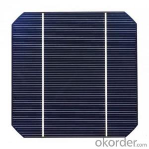
Specifications of Mono Solar Wafer
Monocrystalline solar wafer 125*125mm
Conductivity Type: P type
Dopant: Boron
Resistivity: 1~3 ohm
thickness: 200um.
| Product name | Mono Wafer |
| Conductive type | P type |
| Square size wafer(mm) | 125×125±0.5 mm |
| Resistivity | 1~3 ohm |
| Corner(mm) | 150±0.5;165±0.5 |
| 195±0.5;200±0.5 | |
| Thickness (μm) | 200±20 |
| Total thickness(um) | ≤ 30 |
| Resistivity range(Ωcm) | 1-3 |
| Doping elements | Boron |
| Orientation | (100)±1° |
| Carbon content(atoms/cc) | ≤1.0E+17 |
| Oxygen content(atoms/cc) | ≤1.0E+18 |
| Lifetime(μs) | ≥10 |
| Surface quality | No crack, gap, missing Angle, perforated, silicon fell and stress |
| Warping degrees(warp/μm) | ≤50 |
| Neighbouring vertical degree | 90±0.5° |
| Side damage(mm) | ≤0.5mm(length)×0.3mm(width)(not more than 2 per wafer) |
| Line mark(μm) | ≤15 |
Advantages of Mono Solar Wafers
1. High efficiency and High power.2. Long-term electrical stability.
3. Lowest price and Fastest delivery.
4. Good quality and good service.
5. Bulk supply
6. Good Warranty
7. Big Sale
8. More than 25 years on the lifetime.
Usage and Applications of Mono Solar Wafers
Mono Solar wafers is used to make Solar Cells. With high quality and stable quality. Our Solar Wafers can greatly improve the performance of Solar Cells.
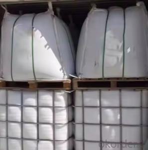
Packaging & Delivery of Mono Solar Wafers
Carton Box Package and Deliver by air.It should be noticed that it should be avoid of water, sunshine and moist.
Wafer Factory Picture of Mono Solar Wafers

Package Picture of Mono Solar Wafers

- Q:What is the role of back contacts on solar silicon wafers?
- The role of back contacts on solar silicon wafers is to provide an electrical connection for the flow of current generated by the solar cells. They are typically made of metal and are placed on the backside of the wafer, opposite to the side exposed to sunlight. Back contacts help in collecting and conducting the electricity produced by the solar cells to the external circuit, enabling the utilization of solar energy for various applications.
- Q:What is the role of interconnection on solar silicon wafers?
- The role of interconnection on solar silicon wafers is to connect individual solar cells together in a series or parallel configuration to form a solar module. This interconnection allows for the flow of electricity generated by the solar cells, enabling the module to produce usable electricity.
- Q:What is the role of edge isolation in solar silicon wafers?
- The role of edge isolation in solar silicon wafers is to prevent any electrical leakage or short circuits between the front and back surfaces of the wafer. By isolating the edges, it ensures that the current generated by the sunlight is channeled efficiently through the front surface and collected by the metal contacts on the back surface, resulting in improved solar cell performance and higher overall efficiency.
- Q:How are solar silicon wafers affected by humidity and moisture?
- Solar silicon wafers are adversely affected by humidity and moisture. Moisture can cause corrosion and oxidation of the wafer's surface, leading to reduced efficiency and performance of the solar cell. High humidity levels can also result in the formation of water droplets on the wafer, which can create shading and impact the generation of electricity. Therefore, it is crucial to protect solar silicon wafers from excessive humidity and moisture to ensure their optimal functioning and longevity.
- Q:What is the size of a typical solar silicon wafer?
- A typical solar silicon wafer is typically around 156mm (6.14 inches) in size.
- Q:Can solar silicon wafers be used in solar-powered remote sensing devices?
- Yes, solar silicon wafers can be used in solar-powered remote sensing devices. These wafers are commonly used to produce photovoltaic cells, which convert sunlight into electricity. By integrating solar silicon wafers into remote sensing devices, they can harness solar energy to power their operations, making them more sustainable and independent from external power sources.
- Q:I would like to ask: silicon annealing treatment is how? Why anneal? Does annealing have an effect on the resistivity and the minority lifetime?
- Silicon wafer annealing process, is a part of the process. According to a certain procedure, the process of heating and cooling..;
- Q:How do solar silicon wafers perform in high pollution areas?
- Solar silicon wafers generally perform well in high pollution areas, but excessive pollution can affect their efficiency and performance. Air pollution, specifically particulate matter and smog, can reduce the amount of sunlight reaching the wafers, resulting in decreased power output. Additionally, pollutants can settle on the surface of the wafers, reducing their ability to absorb sunlight effectively. Regular cleaning and maintenance can help mitigate these effects and ensure optimal performance in high pollution areas.
- Q:What is the cost of manufacturing a solar silicon wafer?
- The cost of manufacturing a solar silicon wafer can vary depending on various factors such as the size, quality, and production volume. However, on average, the cost can range from a few dollars to around $10 per wafer.
- Q:What is the impact of light-induced degradation on the performance of solar silicon wafers?
- Light-induced degradation can have a significant impact on the performance of solar silicon wafers. This phenomenon, also known as LID, refers to the decrease in the efficiency of solar cells after exposure to sunlight. LID occurs due to the formation of defects in the silicon material, which reduce the ability of the solar cell to convert light into electricity. This degradation can result in lower power output and decreased overall performance of the solar panel system. To mitigate the impact of LID, manufacturers employ various techniques such as passivation processes and anti-LID treatments to improve the long-term stability and efficiency of solar silicon wafers.
1. Manufacturer Overview |
|
|---|---|
| Location | |
| Year Established | |
| Annual Output Value | |
| Main Markets | |
| Company Certifications | |
2. Manufacturer Certificates |
|
|---|---|
| a) Certification Name | |
| Range | |
| Reference | |
| Validity Period | |
3. Manufacturer Capability |
|
|---|---|
| a)Trade Capacity | |
| Nearest Port | |
| Export Percentage | |
| No.of Employees in Trade Department | |
| Language Spoken: | |
| b)Factory Information | |
| Factory Size: | |
| No. of Production Lines | |
| Contract Manufacturing | |
| Product Price Range | |
Send your message to us
Monocrystalline Silicon Wafer,125*125, Solar Wafers
- Ref Price:
-
- Loading Port:
- Shanghai Port
- Payment Terms:
- TT or LC
- Min Order Qty:
- 100 Pieces PCS
- Supply Capability:
- 700MW/Per Year PCS/month
OKorder Service Pledge
OKorder Financial Service
Similar products


New products

Hot products


Hot Searches
Related keywords

