
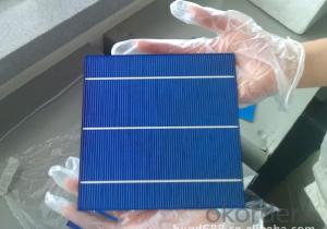
Solar Cell High Quality A Grade Cell Polyrystalline 5v 16.0%
- Ref Price:
-

- Loading Port:
- Shanghai
- Payment Terms:
- TT OR LC
- Min Order Qty:
- 1000 pc
- Supply Capability:
- 100000 pc/month
OKorder Service Pledge
OKorder Financial Service
You Might Also Like


Specifications
hot sale solar cell
1.16.8%~18.25% high efficiency
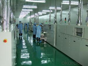
2.100% checked quality
3.ISO9001/ISO14001/TUV/CE/UL
4.stable performance
We can offer you the best quality products and services, don't miss !
POLY6'(156*156)
Polycrystalline Silicon Solar cell
Physical Characteristics
Dimension: 156mm×156mm±0.5mm
Diagonal: 220mm±0.5mm
Thickness(Si): 200±20 μm
Front(-) Back(+)
Blue anti-reflecting coating (silicon nitride); Aluminum back surface field;
1.5mm wide bus bars; 2.0mm wide soldering pads;
Distance between bus bars: 51mm . Distance between bus bars :51mm .
Electrical Characteristics
Efficiency(%) | 18.00 | 17.80 | 17.60 | 17.40 | 17.20 | 16.80 | 16.60 | 16.40 | 16.20 | 16.00 | 15.80 | 15.60 |
Pmpp(W) | 4.33 | 4.29 | 4.24 | 4.19 | 4.14 | 4.09 | 4.04 | 3.99 | 3.94 | 3.90 | 3.86 | 3.82 |
Umpp(V) | 0.530 | 0.527 | 0.524 | 0.521 | 0.518 | 0.516 | 0.514 | 0.511 | 0.509 | 0.506 | 0.503 | 0.501 |
Impp(A) | 8.159 | 8.126 | 8.081 | 8.035 | 7.990 | 7.938 | 7.876 | 7.813 | 7.754 | 7.698 | 7.642 | 7.586 |
Uoc(V) | 0.633 | 0.631 | 0.628 | 0.625 | 0.623 | 0.620 | 0.618 | 0.617 | 0.615 | 0.613 | 0.611 | 0.609 |
Isc(A) | 8.709 | 8.677 | 8.629 | 8.578 | 8.531 | 8.478 | 8.419 | 8.356 | 8.289 | 8.220 | 8.151 | 8.083 |

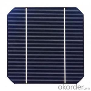
MONO5'(125*125mm)165
Monocrystalline silicon solar cell
Physical Characteristics
Dimension: 125mm×125mm±0.5mm
Diagonal: 165mm±0.5mm
Thickness(Si): 200±20 μm
Front(-) Back(+)
Blue anti-reflecting coating(silicon nitride); Aluminum back surface field;
1.6mmwide bus bars; 2.5mm wide soldering pads;
Distance between bus bars: 61mm . Distance between bus bars :61mm .
Electrical Characteristics
Efficiency(%) | 19.40 | 19.20 | 19.00 | 18.80 | 18.60 | 18.40 | 18.20 | 18.00 | 17.80 | 17.60 | 17.40 | 17.20 |
Pmpp(W) | 2.97 | 2.94 | 2.91 | 2.88 | 2.85 | 2.82 | 2.79 | 2.76 | 2.73 | 2.70 | 2.67 | 2.62 |
Umpp(V) | 0.537 | 0.535 | 0.533 | 0.531 | 0.527 | 0.524 | 0.521 | 0.518 | 0.516 | 0.515 | 0.513 | 0.509 |
Impp(A) | 5.531 | 5.495 | 5.460 | 5.424 | 5.408 | 5.382 | 5.355 | 5.328 | 5.291 | 5.243 | 5.195 | 4.147 |
Uoc(V) | 0.637 | 0.637 | 0.636 | 0.635 | 0.633 | 0.630 | 0.629 | 0.629 | 0.628 | 0.626 | 0.626 | 0.625 |
Isc(A) | 5.888 | 5.876 | 5.862 | 5.848 | 5.839 | 5.826 | 5.809 | 5.791 | 5.779 | 5.756 | 5.293 | 5.144 |

FAQ:
Q:How can i get some sample?
A:Yes , if you want order ,sample is not a problem.
Q:How about your solar panel efficency?
A: Our product efficency around 17.25%~18.25%.
Q:What’s the certificate you have got?
A: we have overall product certificate of ISO9001/ISO14001/CE/TUV/UL
- Q:Can solar silicon wafers be used in solar-powered space vehicles?
- Yes, solar silicon wafers can be used in solar-powered space vehicles. They are commonly used in photovoltaic cells to convert sunlight into electricity, providing a sustainable power source for space missions.
- Q:How are solar silicon wafers handled and transported?
- Solar silicon wafers are handled and transported with great care to ensure their quality and integrity. They are typically stored in cleanroom environments to prevent contamination. When being transported, they are usually packaged in protective materials such as antistatic bags or foam inserts to prevent any damage or breakage. Specialized carriers or trucks equipped with shock-absorbing systems are used to minimize vibrations and impacts during transportation. Additionally, temperature and humidity control measures are implemented to avoid any adverse effects on the wafers. Overall, meticulous handling and secure packaging are essential to maintain the high quality of solar silicon wafers throughout their transportation process.
- Q:How are solar silicon wafers affected by light-induced degradation mechanisms?
- Solar silicon wafers are affected by light-induced degradation mechanisms, specifically due to the presence of impurities or defects in the silicon material. These impurities can create energy levels within the bandgap of the silicon, which can trap charge carriers and reduce the efficiency of the solar cell. Additionally, exposure to sunlight can cause the formation of oxygen-related defects, such as interstitial oxygen, which can further impact the performance of the solar cells. Overall, light-induced degradation mechanisms can lead to a decrease in the power output and efficiency of solar silicon wafers over time.
- Q:Why the resistivity of silicon wafer is high and low
- For example, after heating resistance and cooling, more or less there will be changes in the normal temperature change, is allowed error.
- Q:Can solar silicon wafers be used in solar-powered water treatment plants?
- Yes, solar silicon wafers can be used in solar-powered water treatment plants. These wafers are commonly used in photovoltaic panels to convert sunlight into electricity. In a solar-powered water treatment plant, the solar silicon wafers can be utilized to generate the necessary energy to power the treatment processes, such as filtration, disinfection, and desalination.
- Q:What is the role of doping on solar silicon wafers?
- The role of doping on solar silicon wafers is to introduce impurities into the silicon material, which alters its electrical properties. This process helps create the desired p-n junctions and enables the conversion of sunlight into electricity more efficiently.
- Q:The purpose and means of chemical etching of silicon wafers?
- What are the means of chemical etching of silicon: 1 acid corrosion of 2 alkaline corrosion
- Q:Can solar silicon wafers be used in solar-powered military applications?
- Yes, solar silicon wafers can be used in solar-powered military applications. They are commonly used in various military applications such as powering remote military outposts, surveillance systems, and communication equipment. The durability, efficiency, and versatility of solar silicon wafers make them a viable option for meeting the energy needs of military operations in remote and off-grid locations.
- Q:Geometric parameters and testing of silicon wafer
- Silicon chips have side length 125mm, 156mm, and 125 of the large chamfer diagonal 156mm and small chamfer diagonal 165mm, polycrystalline silicon chip to the side of the 156mm based, diagonal 219.2mm.
- Q:What is the role of oxide layers on solar silicon wafers?
- The role of oxide layers on solar silicon wafers is to act as a passivation layer, preventing recombination of charge carriers and improving the efficiency of the solar cell by reducing surface recombination and enhancing the electrical properties of the wafer.
1. Manufacturer Overview |
|
|---|---|
| Location | |
| Year Established | |
| Annual Output Value | |
| Main Markets | |
| Company Certifications | |
2. Manufacturer Certificates |
|
|---|---|
| a) Certification Name | |
| Range | |
| Reference | |
| Validity Period | |
3. Manufacturer Capability |
|
|---|---|
| a)Trade Capacity | |
| Nearest Port | |
| Export Percentage | |
| No.of Employees in Trade Department | |
| Language Spoken: | |
| b)Factory Information | |
| Factory Size: | |
| No. of Production Lines | |
| Contract Manufacturing | |
| Product Price Range | |
Send your message to us
Solar Cell High Quality A Grade Cell Polyrystalline 5v 16.0%
- Ref Price:
-
- Loading Port:
- Shanghai
- Payment Terms:
- TT OR LC
- Min Order Qty:
- 1000 pc
- Supply Capability:
- 100000 pc/month
OKorder Service Pledge
OKorder Financial Service
Similar products


New products

Hot products


Hot Searches
Related keywords

