


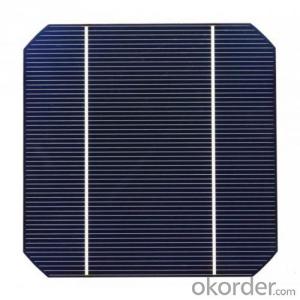
Mono Solar Cells156mm*156mm in Bulk Quantity Low Price Stock 19.2
- Ref Price:
-

- Loading Port:
- Shanghai
- Payment Terms:
- TT OR LC
- Min Order Qty:
- 1000 pc
- Supply Capability:
- 100000 pc/month
OKorder Service Pledge
OKorder Financial Service
You Might Also Like


Brief Introduction
- Up to 20.0% efficiency, one of the highest performing mono crystalline cells on the market
- Three bus bars boosts current collection over the entire cell area, leading to higher fill factors
- Blue anti-reflecting coating allows more sunlight be captured and converted to electricity
- Finer, closer fingers improves charge collections for improved energy yield
- Lower light-induced degradation leads to greater power output over the entire module lifetime
- All solar cells are tightly classified to optimize output of module
- Maximum yield and longevity due to hotspot prevention
- Premium appearance results in a highly uniform and aesthetically appealing module
Specification
- Product Mono-crystalline silicon solar cell
- Dimension 156 mm x 156 mm ± 0.5 mm
- Thickness 200 μm ± 30 μm
- Front 1.5 ± 0.1 mm busbar (silver)
- Silicon nitride antireflection coating
- Back 3.0 mm continuous soldering pads (silver)
- Back surface field (aluminum)
Electric performance parameters

- Testing conditions: 1000 W/m2, AM 1.5, 25 °C, Tolerance: Efficiency ± 0.2% abs., Pmpp ±1.5% rel.
- Imin : at 0.5 V
Light Intensity Dependence

Soldering Ability
- Peel Strength: > 1.0 N/mm (Pull soldered ribbon from busbar in 5 mm/s of 180°)
Dimension Figure

Quick Response
- Any time and anywhere, reply clients' email and solve all problems happen in the work at the first time.
- Remove clients doubts and offer the best solution at the first time.
- Give our clients the lastest news of the photovoltaic, update the newest stock informtion.
Production and Quality Control
- Precision cell efficiency sorting procedures
- Stringent criteria for color uniformity and appearance
- Reverse current and shunt resistance screening
- ISO9001,ISO14001 and OHSAS 18001,TUV Certificated


FAQ:
1. Q: Do you have your own factory?
A: Yes, we have. Our factory located in Jiangsu
2. Q: How can I visit your factory?
A: Before you visit,please contact us.We will show you the route or arrange a car to pick you up.
3. Q: Do you provide free sample?
A: Commenly we provide paid sample.
4. Q: Could you print our company LOGO on the nameplate and package?
A: Yes, we accept it.And need an Authorization Letter from you.
5. Q: Do you accept custom design on size?
A: Yes, if the size is reasonable.
6. Q: How can I be your agent in my country?
A: Please leave feedback. It's better for us to talk about details by email.
7. Q: Do you have solar project engineer who can guide me to install system?
A: Yes, we have a professional engineer team. They can teach you how to install a solar system.
- Q:Can solar silicon wafers be used in remote or isolated areas?
- Yes, solar silicon wafers can be used in remote or isolated areas. Solar panels made from silicon wafers can generate electricity from sunlight, making them an ideal solution for areas where access to traditional power grids is limited or non-existent. The modular nature of solar panels allows for easy installation and scalability, making it feasible to meet the energy needs of remote or isolated communities. Additionally, advancements in battery storage technology enable the storage of excess energy generated during the day for use during nighttime or cloudy periods, further enhancing the viability of solar power in remote areas.
- Q:What is the typical cost per watt for a solar silicon wafer?
- The typical cost per watt for a solar silicon wafer ranges from $0.20 to $0.40.
- Q:How is the weight of a solar silicon wafer reduced?
- The weight of a solar silicon wafer is reduced through a process called wafer thinning. This involves removing a portion of the wafer's thickness, typically through mechanical grinding or chemical etching methods, to make it lighter and more flexible without compromising its functionality.
- Q:How are solar silicon wafers tested for thermal properties?
- Solar silicon wafers are typically tested for thermal properties by subjecting them to a series of controlled heating and cooling cycles. This process involves placing the wafers in a controlled environment and gradually increasing the temperature while monitoring their response. The thermal conductivity, coefficient of thermal expansion, and other relevant parameters are measured to assess the wafers' thermal properties. Additionally, specialized equipment like thermal imaging cameras may be used to detect any hotspots or temperature variations across the wafer's surface during testing.
- Q:What is the role of back surface field on solar silicon wafers?
- The role of back surface field on solar silicon wafers is to enhance the efficiency of the solar cell by reducing the recombination of charge carriers at the back surface. It helps to create a strong electric field at the back surface, which prevents the loss of generated electrons and holes. This improved charge collection increases the overall power output of the solar cell.
- Q:What is the typical thickness tolerance of a solar silicon wafer?
- The typical thickness tolerance of a solar silicon wafer is around ± 20 micrometers.
- Q:Are there any initiatives to reduce the environmental impact of solar silicon wafer production?
- Yes, there are various initiatives aimed at reducing the environmental impact of solar silicon wafer production. These include the development and adoption of more sustainable manufacturing processes, such as the use of renewable energy sources in production facilities, reducing water usage, and implementing recycling programs for waste materials. Additionally, research is being conducted to explore alternative materials and techniques that could further minimize the environmental footprint of solar silicon wafer production.
- Q:Are solar silicon wafers affected by electromagnetic interference?
- Yes, solar silicon wafers can be affected by electromagnetic interference. Electromagnetic interference (EMI) can disrupt the normal functioning of solar silicon wafers by interfering with the flow of electricity or causing fluctuations in the voltage output. To mitigate this, proper grounding, shielding, and EMI protection measures are implemented in solar panel installations to minimize the impact of electromagnetic interference on the performance of silicon wafers.
- Q:How is a front contact applied to a solar silicon wafer?
- A front contact is typically applied to a solar silicon wafer using a screen printing process. The process involves depositing a conductive paste onto the front surface of the wafer through a fine mesh screen. This paste consists of metal particles, such as silver or aluminum, mixed with a binder material. The screen is aligned with the wafer's surface, and the paste is forced through the screen using a squeegee, leaving a patterned layer of conductive material on the wafer. This front contact layer helps to collect and transport the electrical current generated by the solar cells.
- Q:What are the different types of glass covers used on solar silicon wafers?
- There are typically two types of glass covers used on solar silicon wafers: tempered glass and anti-reflective coated glass. Tempered glass is a type of safety glass that is more durable and resistant to breakage. Anti-reflective coated glass, on the other hand, has a special coating that reduces reflection and increases light absorption, maximizing the efficiency of solar cells.
1. Manufacturer Overview |
|
|---|---|
| Location | |
| Year Established | |
| Annual Output Value | |
| Main Markets | |
| Company Certifications | |
2. Manufacturer Certificates |
|
|---|---|
| a) Certification Name | |
| Range | |
| Reference | |
| Validity Period | |
3. Manufacturer Capability |
|
|---|---|
| a)Trade Capacity | |
| Nearest Port | |
| Export Percentage | |
| No.of Employees in Trade Department | |
| Language Spoken: | |
| b)Factory Information | |
| Factory Size: | |
| No. of Production Lines | |
| Contract Manufacturing | |
| Product Price Range | |
Send your message to us
Mono Solar Cells156mm*156mm in Bulk Quantity Low Price Stock 19.2
- Ref Price:
-
- Loading Port:
- Shanghai
- Payment Terms:
- TT OR LC
- Min Order Qty:
- 1000 pc
- Supply Capability:
- 100000 pc/month
OKorder Service Pledge
OKorder Financial Service
Similar products


New products
Hot products


Hot Searches
Related keywords

