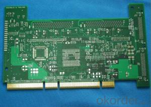


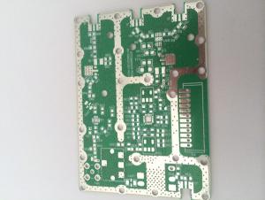
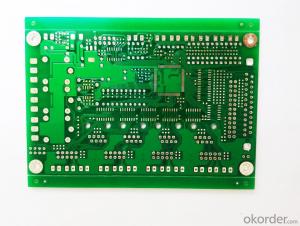
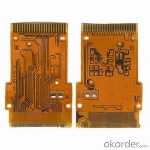
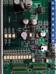
High quality 8 layer gold finger pcb, made in china
- Ref Price:
-

- Loading Port:
- Shanghai
- Payment Terms:
- TT OR LC
- Min Order Qty:
- 1 pc
- Supply Capability:
- 10000 pc/month
OKorder Service Pledge
OKorder Financial Service
You Might Also Like

Item specifice

Product Description
1. UL,ISO9001,ISO14001, TS16949 certificate
2. Short lead time.
3. PCB ROHS compliant.
4. Turkey service
Free Technology Support
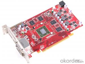
PCB Assembly
Turnkey service(PCB manufacture, components procurement and assembly)
Minimum lead time for assembly is only 5 days
Prototype building, No Minimum quantity Required
Reliable Parts
Surface mount, through hole, BGA, QFP, QFN …
ROHS compliant and lead-free process
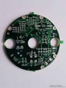
PCB Capability
Material: FR4, CEM-3, Halogen Free, Rogers, High TG etc.
Layer counts: 1-18 layers
Finished Copper Thickness: 0.5-4 OZ
Finished Board Thickness: 0.2-5.0mm
Min. Line/Track Width: 4mil
Min. Line/Track Space: 4mil
Min. Contour Tolerance: +/-0.1mm
Min. Finished Diameter of PTH Hole: 0.2mm
Max. Board Thickness/Hole Ratio: 12:1
Min. Solder Mask Bridge: 4mil (Min. SMT Pad Space 8mil)
Min. Legend (Silk screen) Track Width: 5mil
Min. Legend (Silk screen) Height: 30mil
Min. drilling slot size: 0.6mm
Solder mask color: green, black, blue, white, yellow, purple, and matt, etc.
Legend/Silk screen Color: white, yellow, black, etc.
Surface Treatment: HAL, Lead Free HAL, Immersion gold, OSP, Immersion tin, Immersion silver, etc.
Other Technology: Gold finger, peelable mask, Non-across blind/buried vias, characteristic impedance control, Rigid-flex board etc.
Reliability Test: flying probe test/fixture test, impedance test, solderability test, thermal shock test, hole resistance test, and micro metallographic section analysis, etc.
Bow and twist: ≤1%
Flammability: 94V-0
4. Professional engineering staff to provide technical support.
5.OEM and ODM service are welcome.
Packaging Detail: Vacuum packaging
Delivery Time: 10-15 days
- Q:What is the working principle of the circuit board?
- Circuit board works: the electronic components on the fixed and connected into the circuit. Circuit board name: circuit boards, PCB board, aluminum plate, high frequency board, thick copper plate, impedance board, PCB, ultra-thin circuit boards, ultra-thin circuit boards, printing (copper etching technology) circuit boards.
- Q:Multilayer circuit boards, is not all power must be placed on the inner layer
- The board is divided into single-sided and double-sided, but the high-end electronic products, due to product space design constraints, except for the number of wiring board to determine the difficulty of processing and processing prices, ordinary circuit board points single-sided and double- Surface wiring, the internal stack can be multi-layer lines, the production process, making a good layer of each layer, and then through the optical device positioning, pressure, so multilayer lines stacked in a circuit board. Commonly known as multi-layer circuit boards.
- Q:Protel pcb how to rotate the board?
- spreadsheet generation, support macro operation and other functions, and has Client / Server ( Client / server) architecture, but also compatible with some other design software file formats, such as ORCAD, PSPICE, EXCEL, etc., the multi-layer printed circuit board automatic wiring can achieve high density PCB 100% distribution rate.
- Q:PCB board can be stored for how long
- For example: because there are integrated circuit parts loaded on the circuit board, so the news media called him IC board, but in essence he is not the same as the printed circuit board. We usually say that the printed circuit board refers to the bare board - that is, no components on the circuit board.
- Q:Protel how to lock all components
- running in the DOS environment, the hardware requirements are very low, no hard disk 286 1M memory can run, but its function is less, only the circuit schematic Drawing and PCB design function, the printed circuit board automatic distribution of the cloth rate is low, and today's PROTEL has been developed to DXP 2004, is a huge EDA software,
- Q:Which boards are difficult boards?
- If the circuit board according to the product classification, there are single-sided printed circuit boards, double-sided printed circuit boards, multi-layer printed circuit boards, HDI high-density microporous printed circuit boards, flexible printed circuit boards,
- Q:What is the multilayer circuit board
- In the formation of layers through the hole after the formation of metal copper layer on its need to complete the inter-layer circuit conduction. First with a heavy brush and high pressure flushing the way to clean up the holes on the hole and the hole in the dust, and then to potassium permanganate solution to remove the hole on the copper surface of the glue residue. In the clean hole on the wall soaked with tin palladium paste layer, and then reduced to metal palladium.
- Q:PCB circuit board has several materials?
- steel plate as a mold, in the hot press by high temperature and high pressure forming process Into the. General multi-layer board with the semi-cured film, it is CCL in the production process of semi-finished products (mostly glass cloth impregnated
- Q:Who can tell me printed circuit board in the multi-layer and double-sided panels and the difference between the single-layer, multi-layer between the layers is how the distribution?
- One side of the circuit, multilayer circuit board is between the board through the small hole connecting circuit `you carefully look at the multi-layer board` there are a lot of small holes above those holes in fact there are wires `is connected to a few boards
- Q:What are the parts of the printed circuit board according to the distribution of the conductive layer? What are the parts of the printed circuit board?
- corresponding location need to be a green oil is not covered with bare copper, easy to heat the components and production welding fixed. Shell is a metal exposed devices such as crystal, serial socket, USB seat, etc., it is best to connect the shell and ground to make it a better shield. Do not have holes or traces below the bare metal, as if it were unavoidable to lay a flat area of ??white oil in its corresponding position to avoid short circuits with other networks below it. Such as the circuit board need to operate the function keys such as settings, reset keys
1. Manufacturer Overview |
|
|---|---|
| Location | |
| Year Established | |
| Annual Output Value | |
| Main Markets | |
| Company Certifications | |
2. Manufacturer Certificates |
|
|---|---|
| a) Certification Name | |
| Range | |
| Reference | |
| Validity Period | |
3. Manufacturer Capability |
|
|---|---|
| a)Trade Capacity | |
| Nearest Port | |
| Export Percentage | |
| No.of Employees in Trade Department | |
| Language Spoken: | |
| b)Factory Information | |
| Factory Size: | |
| No. of Production Lines | |
| Contract Manufacturing | |
| Product Price Range | |
Send your message to us
High quality 8 layer gold finger pcb, made in china
- Ref Price:
-
- Loading Port:
- Shanghai
- Payment Terms:
- TT OR LC
- Min Order Qty:
- 1 pc
- Supply Capability:
- 10000 pc/month
OKorder Service Pledge
OKorder Financial Service
Similar products
New products
Hot products
Hot Searches
Related keywords

